
Nanotube


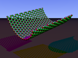
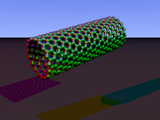
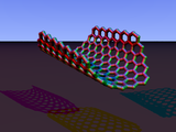
In chemistry, nanotubes refer to tubular (cylindrical) structures whose diameter is one nanometer or less. There are nanotubes made of many materials, such as silicon or boron nitride, but the term is generally applied to carbon nanotubes. Nanotubes have unusual properties, which are valuable for nanotechnology. Depending on the degree of coiling, and the way the original sheet is shaped, the result can lead to nanotubes of different diameters and internal geometry. These are shaped as if the ends of a sheet of paper were joined at their ends to form the aforementioned tube. They are called monolayer nanotubes or single-walled. There are also nanotubes whose structure resembles that of a series of concentric tubes, included one inside the other, logically like matryoshka dolls, with increasing diameters from the center to the periphery. These are multilayer nanotubes. Derivatives are known in which the tube is closed by half a sphere of fullerene, and others that are not closed.
They are being actively studied, like the fullerenes, for their fundamental interest in chemistry and for their technological applications. It is, for example, the first material known to mankind capable, in theory, of indefinitely supporting its own weight suspended from our planet. Theoretically it would make it possible to build a space elevator, since for this a material with a tensile strength of 100 GPa is needed and it is calculated that carbon nanotubes have a tensile strength of 200 GPa.
Types of carbon nanotubes and related structures
Single Wall (SWNT)

Armchair (n,ni.e.: m=n

Translation vector is folded while the chiral vector remains straight

Nanocinta de grafeno
The chiral vector folds, while the translation vector remains straight
Zigzag (n(0.0)

Quiral (n,m)
n and m can be counted at the end of the tube


Most single-walled nanotubes (SWNTs) have a diameter of about 1 nanometer, and can be many millions of times larger. The structure of a SWNT can be conceptualized as the wrapping of an atom-thick layer of graphite, called graphene, in a transparent cylinder. The way to wrap the graphene sheet is represented by a pair of indices (n,m). The integers n and m indicate the number of unit vectors along two directions in the honeycomb lattice of graphene. If m = 0, the nanotubes are called zigzag nanotubes, and if n = m the nanotubes are called armchair nanotubes. If it is the opposite, they are called chiral. A SWNT, for which no additional support is provided, can have a diameter between 0.4 and 6 nanometers and a variable length of up to several micrometers.
Multi-Wall (MWNT)


Multi-walled nanotubes (MWNTs) consist of several laminated layers (concentric tubes) of graphene. There are two models that can be used to describe the structures of multi-walled nanotubes. In the Russian doll model, the graphite sheets are arranged in concentric cylinders, for example, a (0.8) single-walled nanotube (SWNT) inside a larger (0.17) single-walled nanotube. In the parchment model, a single sheet of graphite is wound around itself, resembling a scroll of parchment or a rolled-up newspaper. The distance between layers of multi-walled nanotubes is close to the distance between graphene layers in graphite, approximately 3.4 Å. The structure of the Russian doll is observed most often.
Double-walled carbon nanotubes (DWNTs) form a special class of nanotubes, in that their morphology and properties are similar to those of SWNTs, but their resistance to chemicals is significantly improved.
Torus
In theory a nanotorus is a nanotube folded into a torus (donut shape). Nanotoruses are predicted to have many unique properties, such as magnetic moments 1,000 times larger than previously expected for certain specific radii. Properties such as magnetic moment, thermal stability, etc. vary widely depending on the radius of the toroid and the radius of the tube.
Nanobud

Carbon nanobuds are a newly created material that combines two previously discovered allotropes of carbon: carbon nanotubes and fullerenes. In this new material, the "buds" or "yolks" of fullerene are covalently attached to the outer sidewalls of the underlying carbon nanotube.
This hybrid material has useful properties of both fullerenes and carbon nanotubes. In particular, they have been found to be exceptionally good field emitters. In composite materials, the attached fullerene molecules can function as molecular anchors to prevent nanotube slippage, thus improving the mechanical properties of the composite.
3D nanotube architectures

Recently, several studies have highlighted the possibility of using carbon nanotubes as building blocks to fabricate macroscopic three-dimensional (>100 nm in all three dimensions) all-carbon devices. Lalwani et al. have reported a new thermal crosslinking method to fabricate macroscopic, free-standing, porous, carbon-only scaffolds using single- and multi-walled carbon nanotubes as building blocks. These scaffolds possess macro-, micro-, and nanostructured pores. and the porosity can be tailored for specific applications. These all-carbon 3D scaffolds/architectures can be used for the fabrication of next-generation energy storage, supercapacitors, field emission transistors, high-performance catalysis, photovoltaics, and biomedical devices and implants.
Grafeninated nanotubes (g-CNTs)

Graphenated CNTs are a relatively new phenomenon of hybrids combining graphitic foliates grown along the side walls of multi-walled or bamboo-style carbon nanotubes.
Nitrogen-doped nanotubes
Nitrogen doping plays a key role in lithium storage, as it creates defects in the CNT walls that allow Li ions to diffuse into the interwall space. It also increases capacity, providing more favorable binding of N-doped sites. N-CNTs are also much more reactive to metal oxide nanoparticle deposition, which can further improve storage capacity, especially in materials for lithium-ion battery anodes. However, boron-doped nanotubes have proven to provide batteries with triple the capacity.
Sheath (peapod)
A carbon cladding is a carbon material that traps fullerene inside a carbon nanotube.
Stacked-Cup Carbon Nanotubes
Cup-stacked carbon nanotubes (abbreviated CSCNTs) differ from other near-1D carbon structures, which are normally behave as quasi-metallic conductors of electrons. CSCNTs display semiconductor behaviors due to the stacked microstructures of graphene layers.
Extreme carbon nanotubes

The observation of the longest carbon nanotube grown so far, exceeding 1/2 m (550 mm long), was reported in 2013.
The shortest carbon nanotube is the organic compound cycloparaphenylene, which was synthesized in early 2009.
The thinnest unsustained carbon nanotube is 0.44 nm in diameter. In a stabilizing environment, even smaller diameters can be achieved: up to 0.3 nm for the armchair (2,2) CNT.
Some more information
Properties of nanotubes
Nanotubes usually have a high length/radius ratio, since the radius is usually less than a couple of nanometers and, however, the length can even be 105 nm. Due to this characteristic they can be considered as one-dimensional.
Electrical properties
Nanotubes are characterized by their great electronic complexity, if we take into account the quantum rules that govern electrical conductivity with their size and geometry. These structures can behave, from an electrical point of view, in a wide range of ways, starting with semiconductor behavior up to presenting, in some cases, superconductivity. This wide range of conductivities is given by fundamentally geometric relationships, that is, depending on its diameter, torsion (chirality) and the number of layers of its composition. Thus, for example, there are straight nanotubes (armchair and zigzag) in which the hexagonal arrangements, in the extreme parts of the tube, are always parallel to the axis. This distribution, depending on the diameter, allows two thirds of the non-chiral nanotubes to be conductors and the rest to be semiconductors. In the case of chiral nanotubes, the hexagons have a certain angle with respect to the axis of the tube, that is, the distribution of the lateral hexagons that make up the structure presents a helical winding with respect to the central axis of the tube. This type of conformation makes it difficult for electrons to pass to conduction states or bands, which is why approximately only one third of the nanotubes present appreciable conduction and always as a function of the torsion angle.
It should be noted that superconducting nanotubes could be used for the study of fundamental quantum effects in one dimension, as well as for the search for practical applications in molecular quantum computing. This is because they can act as "quantum conductors", that is, if the voltage is represented, or the potential difference against the current intensity, a straight line is not obtained, but a stepped one. As has been suggested, these structures have a multitude of electrical properties. Regarding the capacity to carry current, it is known that it can reach quantities of approximately one thousand million A/cm², while conventional copper wires melt when reaching current densities of the order of one million A/cm². It should be noted that all these properties do not depend on the length of the tube, unlike what happens in cables in everyday use.
Mechanical properties
If the electrical properties are, in themselves, amazing, the mechanical properties can be even more so. The stability and robustness of the bonds between the carbon atoms, of the sp2 type, gives them the ability to be the most resistant fiber that can be manufactured today. On the other hand, when faced with very intense deformation efforts, they are capable of deform significantly and remain in an elastic regime. The Young's modulus of nanotubes could range between 1.3 and 1.8 terapascals, although to date it has only been possible to obtain experimentally up to 0.8 TPa. In addition, these mechanical properties could be improved: for example in SWNTs (Single Walled NanoTubes), joining several nanotubes in bundles or strings. In this way, even if a nanotube were to break, since they behave as independent units, the fracture would not propagate to the other neighboring ones. In other words, nanotubes can function like extremely firm springs under small stresses and, under larger loads, they can drastically deform and later return to their original shape.
Several studies have tried to measure the mechanical properties and the maximum stress supported by a nanotube, with heterogeneous results, although it could be assumed as a guideline that the maximum stress could be around 150 GPa. This data implies that a 1 cm² thick cable made of nanotubes could support a weight of about 1500 tons. For comparison, an equivalent cable of the best known steel can support 20 tons.
However, not all studies have shown such optimistic values: in general it is commonly accepted that nanotubes are 100 times stronger than steel, and 6 times lighter, even though it is a material little known, these values could vary.
On the other hand, it has been shown that in the radial direction, carbon nanotubes are much less resistant from a mechanical point of view. A complete phase diagram has been produced that gives the transition to a radially collapsed geometry as a function of diameter, pressure, and number of nanotube walls.
Thermal properties
Some models predict that the thermal conductivity of nanotubes can be as high as 6,000 W/mK at room temperature (note, for comparison with another allotrope of carbon, that almost pure diamond transmits 3,320 W/ mK). They are also enormously thermally stable, still stable at 2,800 °C in a vacuum and 750 °C in air (whereas metal wires in microchips are melt between 600 and 1,000 °C). The properties of nanotubes can be modified by encapsulating metals inside, or even gases. In this sense, they would be extraordinary hydrogen stores. As is known, one of the main technical problems for the development of fuel cells is the storage of this element.
Doping
Doping is a technique performed during the synthesis of carbon nanostructures where nanometric particles of some other compatible element can be added for the beneficial alteration of its properties. The main method of its elaboration is by means of CVD. Doping with various elements has been tried and one of the most important that with its properties has helped experimental research is doping with nitrogen.
Timeline of nanotubes
- 1952 First image of carbon nanotubes, published in the Journal of Physical Chemistry of Russia.
- 1991 Official discovery by Iijima (MWCNT).
- 1993 Discovery of the first monolayer nanotube (SWCNT).
- 1991-2000 Product of interest mainly academic.
- 2000-2005 Its industrial use is investigated.
- 2005-2010 Development of industrial applications (projected).
- 2010 Great development of integrated product applications (projected).
Main manufacturing methods
- Laser ablation (High purity, little quantity)
- Voltaic arch download (High purity, little quantity)
- CVD (Chemical vapor deposition) Chemical vapour deposition (great quantity, good quality). The scale increase can be made easily.
Laser ablation
Laser ablation is a process that consists of vaporizing a graphite target through the radiation of a laser pulse, in a high-temperature reactor and in the presence of an inert gas. The nanotubes are formed when the vaporized graphite comes into contact with the cold surface, condensing on the walls of the reactor.
This procedure usually has a typical yield of 70% by weight and produces monolayer nanotubes with a diameter that can be controlled by varying the temperature inside the reactor.
Arc Discharge

Since 1991, the presence of nanotubes has been observed in the soot produced by causing an electric arc between two graphite electrodes. The typical current to produce such an arc was around 100 amps and, paradoxically, what was intended was to produce fullerenes. The first time that carbon nanotubes were produced, in a massive way, was using a method similar to the previous one, by two researchers from the Basic Research Laboratory of the NEC company.
In this process it was observed that the carbon contained in the negative electrode sublimated due to the very high temperatures produced by the discharge that caused the voltaic arc. This technique is the most important method used in the synthesis of nanotubes, since it was the first in which the production of this allotropic form was appreciable.
Arc discharge is a type of continuous electrical discharge that generates very intense light and heat. It is produced between two facing electrodes within a low pressure inert gas atmosphere. An intense current (hundreds of amperes) is passed through the graphite electrodes, which sublimates the carbon atoms from the surface of the electrodes, forming a plasma around them. In an arc open to air, and at normal pressure, (one atmosphere) the positive electrode reaches a temperature of about 3,000 °C.
The typical yield, using this technique, is of the order of 30% by weight and the products obtained are both monolayer and multilayer nanotubes with a typical length of about 50 microns
It can be combined with the purification method, by oxidation, developed by Ebbesen in 1994, which consists of heating the extracted fullerite after discharge at 1,000 K, in an oxygen atmosphere for 30 minutes.
This procedure makes it possible to evaporate the different classes of fullerenes and leave the isolated nanotubes. It is also used to evaporate the outermost walls of multilayer type nanotubes and also to open their ends.
CVD

Catalytic vapor deposition, or Chemical vapor deposition, (hereinafter, CVD) was first described in 1959, but it was not until 1993 when nanotubes could be synthesized using this process. In 2007, a group of researchers from the University of Cincinnati developed a growth process that made it possible to obtain arrays of aligned carbon nanotubes, with an average length of about 18 mm.
In CVD, a substrate is typically prepared with a metal layer, such as nickel, cobalt, gold, or a combination of these. Metal nanoparticles can also be produced by other means, including oxide reduction or solid oxide solutions. The diameters of the nanotubes to be formed, by controlled growth, are related to the size of the metal particles. This size can be controlled by deposition of metal patterns (or masks), or by the addition of etched water onto the metal layer. The substrate is heated to approximately 700 °C.
To start the growth of nanotubes, two gases are mixed in the reactor. A process gas (such as ammonia, nitrogen, hydrogen, etc.) and another gas that is used as a carbon source (such as acetylene, ethylene, ethanol, methane, etc.). The nanotubes grow on the side of the metal catalyst. The carbon-containing gas breaks up on the surface of the catalyst particles, and the carbon is transported to the particle boundaries, where nanotubes are formed. This mechanism is still in the study and discussion phase. The catalyst particles can remain on the growing tips of the nanotubes during the growth process, or continue on the nanotube base, depending on the adhesion between the catalyst particles and the substrate.
CVD is a very common method for the commercial production of carbon nanotubes. For this purpose the metal nanoparticles will be carefully mixed with a catalyst support (for example MgO, Al2O3, etc.) to increase the specific surface area., for the sake of a greater production of the catalytic reaction of feedstock with the metal particles. Another issue of the synthesis route is the removal of the catalytic support by acid treatment, which could sometimes lead to the destruction of the original structure of the nanotubes. Some alternative catalyst supports, which are soluble in water, have been shown to be more effective for nanotube growth.
If a plasma is generated, by applying a strong electric field, during the growth process (plasma-enhanced chemical vapor deposition), then the growth of the nanotube will follow the direction of the electric field.

By properly adjusting the reactor geometry, it is possible to synthesize vertically aligned nanotubes (for example, perpendicular to the substrate), a morphology that has been of interest to researchers interested in electron emission from nanotubes.
Usually, without the presence of plasma, the resulting tubes are randomly oriented. The result is similar to a bowl of carbon spaghetti. Under certain reaction conditions, even in the absence of electric fields, or plasmas, the nanotubes will grow closely spaced and maintain a vertical growth direction. The result is a dense matrix of reassembled tubes, like a carpet or a forest.
Of the methods developed for the synthesis of nanotubes, the CVD technique shows the most promise for the industrial scale in terms of price/unit ratio. There are additional advantages to the synthesis of nanotubes by CVD. Of the different methods for obtaining nanotubes, CVD is the only technique capable of achieving growth directly on a given substrate. However, in the other techniques, the nanotubes must be collected later. The growth sites are controllable by careful deposition of a catalyst. Furthermore, no other growth methods have been developed to produce vertically aligned nanotubes as of yet.
In 2007, a group from Meijo University developed a CVD technique for growing carbon nanotubes from camphor. Another group of researchers from Rice University has concentrated on designing methods for the production of appreciable quantities of nanotubes of great length and purity of a particular conformation. The way to tackle the problem is based on growing long fibers from the seeds that come from a single cut nanotube. In the analysis of the samples it was verified that all the resulting fibers turned out to be of the same diameter and type of the original nanotube. Later, an improvement in the production and length of the nanotubes is expected so that they can be used in industrial applications. CVD growth of multilayer nanotubes is currently used by a few companies to produce tons of materials, including: Arkema, Bayer, Hyperion Catalysis, Mitsui, Nanocyl, NanoLab, Nanothinx, and Showa Denko.
Applications
Electrochemicals
An important application of nanotubes, given their large surface area and low resistivity, is the electrochemistry, such as the development of supercapacitors, hydrogen storage devices, and manufacturing of solar cells.
Supercapacitors
A supercapacitor essentially consists of two carbon electrodes separated by a permeable membrane of ions immersed in an electrolyte. The function of a supercapacitor is measured in terms of the power and of the stored energy density. SWNTs have the highest surface area to volume ratio of any material of carbon, so that its atoms are those that form the surface of the electrode. Currently, supercapacitors are made of activated carbon, which is extremely porous and has a large surface area. In this kind of carbon obtained, the pores are irregular in size and shape, thus reducing the efficiency. In contrast, the vertically aligned CNTs in the supercapacitor have very regular shapes and a width on the order of several diameters. atoms while presenting less resistance, which increases their energy density.
Nanotube-enhanced supercapacitors (both single- and multi-walled) combine the long life and high power of commercial supercapacitors with the higher storage density of chemical batteries. Therefore, they can be used in many energy storage applications.
Hydrogen storage
The large surface area and tubular structure of CNTs make them useful for hydrogen storage. Hydrogen is added to the nanotubes by chemisorption, since the carbon bonds that form the nanotube offer capacity until their saturation incorporating hydrogens. X-ray spectroscopy analysis reveals a decrease in resonance for C-C bonds, and an increase in intensity for C-H bonds.
In the absorption spectrum you can see a peak corresponding to non-hydrogenated carbon, which appears at higher energy, and another peak due to hydrogenated carbon with lower energy. The ratio between the two peaks indicates the amount of hydrogen absorbed, close to that required to be accepted as a vehicle hydrogen storage device.
For example, the Barcelona Institute of Materials Science (ICMAB) is working on it. The idea consists of depositing nanotubes inside a pressure chamber. Hydrogen is allowed to enter said chamber and after a while it is allowed to come out of it. The amount of outgoing gas is less than the incoming. Therefore, it is believed that the hydrogen is incorporated into the nanotube.
Working on this idea, the hydrogen absorption capacity of different nanotube structures has been verified. Thus, a package of double-walled carbon nanotubes (DWNTs) can absorb up to twice as much as SWNTs. From the comparison of the graphite planes of SWNTs, with extreme purity, uniformity and barely traces of impurities, and of DWNTs, with a high ordering, but with lighter packing, in a hexagonal set, it has been found that the latter they present a greater stability for the absorption of H2. This is due to the fact that the nanotube matrix presents pores to which H2 molecules can bind, and given their accessibility and the deeper molecular potential resulting from the overlapping of molecular potentials by the double wall, the absorption is much higher, despite having an area 40% smaller than SWNTs.
Solar cells
Thanks to the unique electrical properties of nanotubes, it is believed that they can be effective in the conversion from solar energy to electricity. The first step in building a solar cell is to assemble carbon nanotubes on a substrate that would act as an electrode, forming a thin layer. Commercially obtained nanotubes are solubilized in a suspension that is transferred to an electrophoresis cell with two parallel transparent optical electrodes (OTEs). By applying a direct current voltage, the suspended nanotubes move towards the positive electrode. By maintaining this voltage for a certain time, the deposition of a SWNT layer on the electrode surface is achieved. You can modify the shape of the layer. For example, if the electrophoresis time is prolonged, the thickness of the layer is increased, or if fields higher than 100 V/m are applied, an alignment of the nanotubes perpendicular to the electrode surface is obtained.
Two ways can be used to use nanotubes in solar cells, either directly excite the semiconductor nanotubes, or use them as conduits to enhance charge transport in nanoassembled light collectors.
In the first case, research is being done with semiconductor SWCNTs, whose electrical properties have been previously detailed. Recent studies have confirmed that nanotubes have a band structure that allows the formation of electron-hole pairs and their subsequent separation by light excitation. The next step is to be able to use these carriers to obtain a current, just as it happens in photovoltaic applications of other semiconductors. Using the layer of nanotubes deposited on the OTE as a photosensitive electrode, a photoelectrochemical cell can be built. An electrolyte is placed between the carbon nanotube layer of the electrode and a platinum foil. The incident light excites the SWNTs and generates charge carriers, after which current generation is observed. This current is cathodic, indicating that the photogenerated holes are accumulated on the OTE surface and transported to the collecting electrode by an external circuit. The present redox reaction makes it possible to recover the charges from the electrode surface in such a way that a constant photocurrent is maintained. The observation of this type of cathodic current assumes that the SWNTs used possess p-type semiconductor properties.
The photoconversion efficiency (IPCE) is measured as the photon-carrier efficiency and is obtained by measuring the photocurrent at different wavelengths. The maximum value obtained by this method is 0.15% at 400 nm, when the usual value in solar cells is around 80-90%. These results can be improved by incorporating a sheet of tin oxide (SnO2) in the OTE which increases the area to collect carriers. Also, through the use of stacked-cup nanotubes (SCCNTs), which present holes in their structure, offering a long portion of edge reagents on the inner and outer surface, and which minimize the interaction between nanotubes by remaining separated in the deposition. on the electrode.
In an OTE/SnO2/SCCNT electrode, the photogenerated electrons in the SCCNT are collected by the SnO2 crystals, generating an anodic current. Therefore, they present an n-type behavior opposite to that of the SWNT layers, with which an IPCE of almost 17% is achieved. The dopants introduced during the synthesis of the nanotubes will mark their p- or n-type properties.
Another procedure that is under development is the use of nanotubes as anchors for nanoassembled light collectors (e.g. semiconductor particles) providing a pathway for the capture of photogenerated charges and their transport to the electrode surface. A very interesting example is the CdS-SWNT composite material that is capable of generate a photocurrent from visible light with high efficiency. The SWNTs layer is deposited on the OTE using the electrophoresis method described above. The electrode is immersed in a solution containing cadmium (Cd) and sulfur (S) ions to form cadmium sulfide (CdS) crystals. The observed anode current confirms that the electrons travel from CdS to the collector electrode through the SWNT network.
As can be seen, and due to the low efficiency shown so far, the introduction of nanotubes in solar cells is still in the experimental phase, in search of better performance.
Electronics
Among the many applications of carbon nanotubes, perhaps the most interesting are in the field of electronics, since they can play the same role as silicon in electronic devices but on a molecular scale, where semiconductors They stop working.
In addition, because the advances in the electronics industry are based on the miniaturization of the devices, which entails an increase in the performance of the processing speed and the density of the circuits, it will be necessary to use carbon nanotubes in their manufacturing. Carbon nanotubes can be used to manufacture multiple devices, including transistors and computer memories.
Transistors
In the field of transistors, semiconductor SWNTs can be inserted between two electrodes (source and drain) in field effect transistors (FETs), called CNTFETs, to create a “highway” for the circulation of electrons. That current can be turned on, or off, by applying a small voltage to the gate, which causes the nanotube's conductivity to change by a factor greater than 106, comparable to silicon FETs. As a result, CNTFETs would switch without error and consume less power than a silicon device. In addition, switching speeds can reach terahertz, which means switching 104 times faster than current processors.
Memories
Other devices that could experience great advances with the introduction of carbon nanotubes in their construction is, without a doubt, random access memory (RAM). Taking into account that the characteristics of an ideal memory of this type would be a large storage capacity, fast and random access to data, low power consumption, low price per stored bit, easy integration into integrated circuit technology and, if possible, the non-volatility of the data after turning off the computer, attempts have been made to design memories whose operation carbon nanotubes play an essential role.
One of the ideas, and perhaps the most important, has been carried out by the group of researchers led by Charles M. Lieber of Harvard University. The design of this memory is based on the elastic properties of nanotubes, which would operate as electromechanical switches. These could be dissected individually.
Another alternative to create a memory would be to think of a nanomechanical device based on a fullerene incorporated into a short carbon nanotube that could be directed to two stable positions, at the ends of it, by means of application of an electric field, although this idea has not yet been applied to any device.
There is another type of memory that combines metallic nanotubes and semiconductors separated by an ONO-type dielectric (SiO2/Si3N4 /SiO2).
Notably, carbon nanotubes can be used to improve other devices such as interconnects or integrated circuits.
Nanotubes in medicine
Bones
"According to the results of an investigation carried out by a team of scientists from the University of California, its organic nature, strength, flexibility and low weight of carbon nanotubes mean that they could serve as scaffolds capable of supporting to bones and help victims of osteoporosis and broken bones. The scientists describe their discovery in a paper published by the American Chemical Society's journal Chemistry of Materials. The results could mean greater flexibility and strength of artificial bones and prostheses, as well as advances in the treatment of the disease osteoporosis. According to the editor of the journal, the research is important because it indicates a possible path for the application of carbon nanotubes in the medical treatment of broken bones. Currently, artificial bone structures are made using a wide variety of materials, such as polymers or peptide fibers, but they have the disadvantage of lacking strength and the risk of being rejected by the human body. However, carbon nanotubes are exceptionally strong, and there is less chance of rejection due to their organic nature. Bone tissue is a natural composite of collagen fibers and crystalline hydroxyapatite, a calcium phosphate-based mineral. The researchers have shown that carbon nanotubes can mimic the function of collagen and act as a scaffold to induce the growth of hydroxyapatite crystals. By treating the nanotubes chemically, it is possible to attract calcium ions which promotes the crystallization process and improves the biocompatibility of the nanotubes by increasing their water solubility."
Nerve cells
Researchers from Italian universities have reportedly grown nerve cells on substrates covered by networks of carbon nanotubes and found an increase in the neural signal transferred between cells. Because CNTs are similar in shape and size to nerve cells, they can help restructure and rewire damaged neurons.
Gene therapy
"Carbon nanotubes offer new gene therapy techniques thanks to the latest scientific advances in medicine, many of the genes related to certain diseases have been identified, and currently research is using this new knowledge to develop new treatments for these diseases. It is believed that defective or missing genes could be replaced through implantation in human cells with the same type of gene. This process is not easy because, since DNA cannot cross the cell membrane, it requires the help of a transporter. Examples of this type of transporter include a virus, a lysosome, or a special peptide. A European team of researchers has developed a new method to introduce DNA into mammalian cells via modified carbon nanotubes. To use nanotubes as gene carriers, it was necessary to modify them. The team of researchers managed to link to the outside of the carbon nanotubes several chains made of carbon and oxygen atoms whose side consists of a group of positively charged amines (– NH3+). This small alteration makes the nanotubes soluble. Also, positively charged groups attract negatively charged phosphate groups on the DNA backbone. By using these attractive electrostatic forces, the scientists were able to solidly attach plasmids to the outside of the nanotubes. They then contacted the nanotube-DNA hybrids with their cell culture of mammalian cells. The result was that the carbon nanotubes, along with their cargo of DNA, entered the cell. Electron microscope images showed how the nanotubes penetrated the cell membrane. Nanotubes do not harm cells because, unlike previous gene transport systems, they do not destabilize the membrane upon penetration. Once inside the cell, the genes turned out to be functional. The use of carbon nanotubes as a carrier will not be limited to gene transplantation. New scientific advances will make possible the transport of medicines and the development of other new medical techniques".
Other industrial applications
By adding small amounts of nanotubes to polymers, they change their electrical properties and this gives rise to the first industrial applications:
- Cars: Antistatic fuel hoses and plastic parts for electrostatic spray paint
- Aerospace: Parts of aircraft
- Packaging: Antistatic for electronics
- Driving ink
- Extremely black materials: The darkest known substance, to date, has been created from carbon nanotubes. The material was manufactured a low density carbon nanotubes matrix, arranged vertically. The material reflection index is three times lower than it had been achieved so far. This "forest" of carbon nanotubes is very good at absorbing the light, but very bad to reflect it. The group of U.S. researchers, belonging to the Rensselaer Polytechnic Institute of Troy, New York, which has developed it ensure that it is the most similar thing to the black body. An ideal body that absorbs light from all wavelengths and from all possible angles. The development of these materials is expected to have applications in the fields of electronics, invisibility in the area of the visible, and in the field of solar energy.
- Sports: Due to the high mechanical resistance of the nanotubes, they are beginning to be used to make tennis rackets stronger, bicycle handlebars, golf clubs, and state-of-the-art arrows.
As adsorbents
Carbon nanotubes have a high surface area, their porous and layered structure is ideal for storing various elements and chemicals.
In recent studies, nanotubes have been adsorbents of: nicotine and tar from cigarette smoke, reactive inks, volatile organic compounds (n-pentane, n-hexane, n-heptane, n-octane, n-cyclohexane, benzene, trichlorethylene), microcystins, divalent metal ions and Trihalomethanes from water (CHCl3, CHBrCl2, CHBr2Cl and CHBr3 ).
- Heavy metal removal: Among the adsorbents of toxic metal ions (activated carb, zeolites, biomaterials, resins, among others) the researchers are interested in the CNTs due to their high absorption capacity. This process has been studied with some divalent ions like: Ni2+, Cu2+, Pb2+Cd2+, Zn2+Co2+.
In studies, nanotubes have shown great potential in adsorption, their future applications are projected in environmental care; in the removal of toxic ions from wastewater from industrial processes.
To improve adsorption efficiency, the nanotubes are subjected to prior oxidation. The oxidation has been done with solutions of various chemical agents such as: KMnO4, HNO3, NaOCl, HCl, H2SO 4, O3, or H2O2; they increase the number of oxygen-containing functional groups (C=O, COOH, OH) and raise the negative surface charge. Oxygen atoms increase the ionic exchange capacity.
Sensors based on carbon nanotubes
Their physicochemical properties make them very sensitive.
- Chemical sensors: due to their characteristic of varying their electrical properties, such as resistance and capacity, by reacting chemically with the substances to be detected.
- Mechanical sensors: are used to discover forces. Due to their piezorresistive qualities, small displacements occur in their atomic structure and their electrical properties are altered.
- Thermal sensors: its resistance changes with temperature, in addition to being pyroelectric.
Opening of nanotubes to obtain graphene
Carbon nanotubes can be opened by different methods in order to form two-dimensional sheets of graphene with a width equivalent to tens of nanometers and the thickness of a carbon atom.
The first method was developed by the American chemist James Tour of Rice University in Houston, who commented in an interview: "The ribbon-shaped carbon structures are very important and are not easy to prepare."
To cut graphene sheets into rings, the first techniques developed use chemicals or ultrasound, but ribbons cannot be prepared in large quantities or with controlled width. Looking for a solution, James Tour, together with a group of researchers led by Hongjie Dai from Stanford University in California, decided to try to make carbon nanotubes by an innovative technique. Using an etching technique, Dai and his colleagues cut the nanotubes from a technique used in the semiconductor industry. The ribbons generated from the carbon nanotubes were deposited on a polymer film that was then removed using gas. ionized argon that helps its thermal disintegration; once cleaned, the remaining nanoribbons are 10 to 20 nanometers wide.
On the other hand, Tour's group used a combination of potassium permanganate and sulfuric acid to extract the tubes open along a single axis. The result was wider nanoribbons (100-500 nm), but without the characteristic properties of a semiconductor, although easier to produce in bulk.
The two techniques are equally useful for research, and both have many potential applications.
Methods for obtaining graphene
Opening of Nanotubes by means of thermal nitrogen expansion: graphene nanocylinders with atomically smooth edges
New physicochemical technique to produce highly crystalline nitrogen-doped graphene nanoribbons.
The technique involves an abrupt expansion of nitrogen gas (N2) within the hollow core of nitrogen-doped multi-walled carbon nanotubes (CNX - MWNT) when exposed to rapid thermal shock. Through theoretical calculations of molecular dynamics and computational simulations, it is possible to propose a mechanism that explains the opening of multi-walled nanotubes by this technique.
When producing nanocylinders with this method, they can be of few layers and can be found both in crystalline zigzags and in armchair edges.
When comparing this technique with the previous ones, we find the following advantages:
- Tubes are not heavily oxidized.
- Atomic sharp edges are produced within nanocinths.
- The technique can be expanded for the bulk production of nanocintas.
The Mexican physicist from Mauricio Terrones (who then worked at the Potosí Institute for Scientific and Technological Research and today is at the Pennsylvania State University) commented on this: “The techniques (developed by Tour and ours) complement each other each other.”
Exfoliated multi-walled carbon nanotubes (MWNTs): graphene sheets and ribbons produced by lithium intercalation and exfoliation of carbon nanotubes
Multi-walled carbon nanotubes (MWNTs) can be opened longitudinally by lithium-ammonia intercalation followed by exfoliation. By interspersing open tubes and exfoliation with acid treatment and abrupt heating, the best results are obtained.
The resulting material is composed of:
- The structures of several flat layers of graphite (nanocintas).
- Multi-wall carbon nanotubes partially open.
- Grapheno cuffs. We call the nanotubes completely unpacked ex MWNTs and their large number of edge atoms makes attractive for many applications.
Mass production of a new form of sp2 carbon: crystalline graphene nanoribbons
The use of the chemical vapor deposition (CVD) technique has been very successful for the mass production (grams per day) of long, thin, and highly crystalline (<20 to 30 microns in length) that have widths of 20 to 300 nm, with small thicknesses (2-40 atomic layers). These layers generally exhibit perfect ABAB stacking arrangements, as occurs in graphite crystals. The structure of the ribbons have been carefully characterized by various techniques, the electron transport and gas adsorption properties have been measured. With this material available to researchers, it should be possible to develop new applications and physicochemical phenomena associated with graphene layers.
Contenido relacionado
Driver
Monomer
Guanine